NOT Gate – Digital Inverter Logic Gate
Binary Logic
Binary logic as the name suggests is a logic represented by two valued number that can be either “0” or “1”. “0” or “1” in binary logic is just a mere illustration of the voltage level.
These terms also used in binary logic gates and circuits
0 or 1
Low or High
True or False
ON or OFF
In TTL logic family, 0 to 0.8 volts is described as “0” or “low state” being low voltage and 2 to 5 volts is described as “1” or “HIGH state” being high voltage.
In CMOS, 0 to 1.5 volts is represented by “0” or “low state” and 3.5 to 5 volts is represented by “1” or “high state”.
Low voltage low state being referred as “0” and high voltage high state being referred as “1”, this representation is your choice.You can cross-represent these two states. Because of this freedom of illustration, there are two logic systems.
Positive Logic
In positive logic, LOW state or low voltage is represented by “0” and High state or high voltage is represented by “1”. it’s additionally referred to as Active HIGH. Usually, this system is used in designing digital circuit.
Negative Logic
In negative logic, LOW state or low voltage is represented by “1” and HIGH state or high voltage is represented by “0”. it’s additionally referred to as Active LOW. This system is used in designing active low digital circuits.
What is Logic NOT Gate?
Logic NOT gahttps://en.wikipedia.org/wiki/Programmable_logic_controllerte is a single input single output Logic gate, that takes Binary Logic (“LOW state” being referred as “0” and “HIGH state” being referred as “1”) as input and produces binary logic as output.
A logic NOT gate takes HIGH state “1” or LOW state ”0” as an input, and produces LOW state “0” and HIGH state “1” respectively as an output. It is also known as a digital inverter because of its inverting property. It inverts (complements) its input signal into the output.
When the input is LOW state “0”, the output is High state “1”. When the input is High state “1”, the output is Low state “0”.
Symbol and Boolean Expression for NOT Gate:

If IN is the input and OUT is the output, then if IN = 0, then OUT = 1
If OUT = 1, then IN = 0.
in other words,
Ā = A
It shows, “If Ā is True, then A is not true”. Or Ā is the inverse of A.
Symbol of NOT Gate:
There are 3 types of symbols used for NOT gate all over the world.
American National Standards Institute (ANSI)/ MILITARY

International Electrotechnical Commission (IEC)/EUROPEAN

Deutsches Institut für Normung (DIN)/GERMANY

Truth Table of NOT Gate:
A mathematical table used to specify input to output logic combination of a digital circuit is known as a truth table, the truth table of NOT Gate is given below

Logic Flow Schematic Diagram of NOT Gate:

Construction and Working Mechanism of NOT Gate:
NOT Gate using Resistor-Transistor Logic
In Resistor-transistor Logic (RTL), bipolar junction transistor (BJT) is used as a switching unit. The schematics of NOT Gate is given in below figures. The first one is an INVERTER made of NPN Transistor and the second one is made up of PNP transistor.
NPN Transistor is active HIGH, which means it will activate once its base input IN is high. Once it’s switched ON, it will conduct current. And voltage drop on OUT will be 0 volt, in other words,GND”0” will flow out as output. When the input is LOW the BJT will switch-OFF, and Vcc”1” will flow out as output.
PNP Transistor is active LOW,which means it will activate when the input IN is LOW. When it’s switched ON Vcc “1” will flow out as output. When input IN is HIGH, PNP BJT will switch-OFF and GND”0” will flow out as output.
Both schematics give the same result, it inverts the input signal.


NOT Gate using MOS Logic (CMOS Transistor as Inverter)
In MOS Logic, MOSFETs are used as switching units,which is controlled by binary input “0” and “1”. Schematic of a NOT gate is shown in the figure given below.
Its working principle is same as RTL logic. NMOS switches on with HIGH input and switches-OFF with LOW input. The output of this circuit will be high “1” when the input is low “0” because NMOS will be switched on and GND ”0” will flow directly to the output.the other case is when the input is HIGH ”1” as a result of which NMOS will switch-OFF and Vdd”1” will flow through OUTPUT.

NOT Gate From Other Logic Gates:
NOT gate function can even be achieved with the help of universal LOGIC gates. NAND gate and NOR gate are Universal logic gates because they can be used instead of any logic gate. They can be used as NOT gate/INVERTER if we combine its input lines into a common input line as shown in the figure given below.
NOT Gate using NAND Gate
NAND gate gives output high when both of the inputs are low and provides an output low when both of the input is high.Such is the case with NOT gate but it has a single input so we combine NAND gate input into a common input line.

The Boolean expression for the NAND used NOT gate is given below:
NOT Gate using NOR Gate
Similarly,NOR gate gives high state when both of the inputs are a LOW state, and gives LOW state when both of the input is high,we can say it’s a NOT gate.

The Boolean expression for the NOR used NOT gate is given as
Output (OUT) = NOT (IN + IN)
TTL and CMOS Logic NOT Gate IC’s
CMOS Logic NOT Gates
- 4000 – Dual 3-input NOR gate + 1 NOT gate
- 4007 – Dual complementary pair + 1 NOT gate
- CD4009 Hex Inverting NOT Gate
- 40106 – Hex inverting Schmitt trigger-(NOT gates)
- CD4069 Hex Inverting NOT Gate
- 4572 – Hex gate, quad NOT, single NAND, single NOR
TTL Logic NOT Gates
- 74LS04 Hex Inverting NOT Gate
- 74LS05 Hex NOT (with open collector outputs)
- 74LS14 Hex Schmitt Inverting NOT Gate7
- 4LS1004 Hex Inverting Drivers
7404 NOT Gate or Inverter IC
Commonly used NOT gate DIP (dual in-line package) IC is 7404 (7404 Hex Inverter NOT Gate) having 6 discrete NOT gates operating on TTL voltages. It has 14 pins and its configuration is given below.


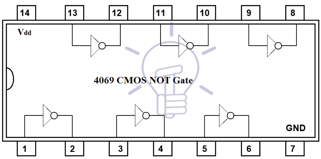
4069 CMOS NOT Gate IC
4069 is CMOS NOT gate IC with same pin description as TTL.

| Pin Number | Configuration |
| 1 | Input 1 |
| 2 | Output 1 |
| 3 | Input 2 |
| 4 | Output 2 |
| 5 | Input 3 |
| 6 | Output 3 |
| 7 | GND |
| 8 | Output 4 |
| 9 | Input 4 |
| 10 | Output 5 |
| 11 | Input 5 |
| 12 | Output 6 |
| 13 | Input 6 |
| 14 | Vcc, voltage supply +5v |
Not Gate Applications
NOT gates also known as inverters due the inverting capabilities of the input i.e. if the input is “0”, the output will be “1” and vice versa.
Some common application and uses of Not gate are:
- They are widely used in digital electronic circuits due to low power consumption
- CMOS inverters are used in oscillators (sine to square wave converters as square wave clock signals) because they can be easily interacted than other logic gate circuits.
- It is used in calculators, computers and common digital logic circuits.
