4 Bit Serial Adder
Serial Adder performs the addition operation bit-by-bit , therefore it requires only one full adder irrespective of number of bits to be added.The serial adder requires simpler circuitry than the parallel adder but the speed of serial adder is relatively smaller.
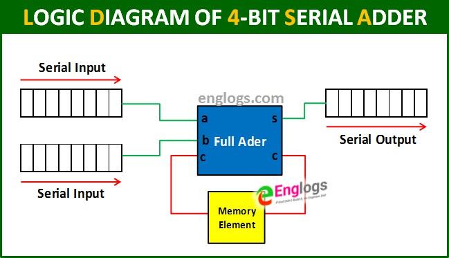
LOGIC DIAGRAM OF 4-BIT SERIAL ADDER:

Above figure shows the diagram of 4-bit serial adder. It consists of two shift right registers A and B , which stores the number to be added serially. Full Adder adds the one pair of bits and carry input at a time. A D-flip flop is used to store the carry output of the full adder and output of the D-flip flop is connected to the carry input of the full adder.
WORKING OF 4- BIT SERIAL ADDER:
For each succeeding clock pulse, the contents of the shift registers A and B shifts from left to right and the Sum bit from the full adder are transferred to the “Sum Register”(as shown in fig). While the carry output from full adder is transferred to the D flip-flop and its output drives the carry input of the adder.
Consider the following example. Let the number (A₃A₂A₁A₀) be 0111 and number(B₃B₂B₁B₀) be 0010, stored in shift registers A and B respectively. Also the carry flip-flop has been initially cleared i.e, Cin = 0.
First Clock Pulse – Before the first clock pulse, the inputs to the full adder are A₀=1 and B₀ = 0 and Cin=0. Output of the full adder are S = 1 and Cout = 0. When the first clock pulse occurs, the values present in A and B registers shift from left to right by one bit. In addition to this, the sum is transferred to the S₃ of the “Sum Register” and the Cout is transferred to the D flip-flop and its output becomes 0.
Second Clock Pulse – Now the input to the full adder becomes A₁ = 1 and B₁ = 1 and Cin = 0, because the output of D flip flop during first clock pulse is 0. The output of full adder are S=0 and Cout=1. When the second clock pulse occurs ,the values present in A and B registers shift from left to right by one bit. In addition to this, the sum is transferred to the S₃ of the “Sum Register” and the Cout is transferred to the D flip-flop and its output becomes 1.
Third Clock Pulse – Now the input to the full adder becomes A₂ = 1 and B₂ = 0 and Cin = 1, (because the output of D flip flop during second clock pulse is 1). The output of full adder are S=0 and Cout=1. When the third clock pulse occurs ,the values present in A and B registers shift from left to right by one bit. In addition to this, the sum is transferred to the S₃ of the “Sum Register” and the Cout is transferred to the D flip-flop and its output becomes 1.
Fourth Clock Pulse – Now the input to the full adder becomes A₃ = 0 and B₃ = 0 and Cin = 1, (because the output of D flip flop during first clock pulse is 1). The output of full adder are S=1 and Cout=0. When the fourth clock pulse occurs, it transfers the S=1 to S₃ of the “Sum Register”. At the end of the fourth clock pulse, the sum value is (1001) will be available in the sum register and Cout is 0.
Hence, in this way serial adder works.


Pingback: Registers and Shift Registers :: Definition, Function & Examples